
U of S research advances materials science
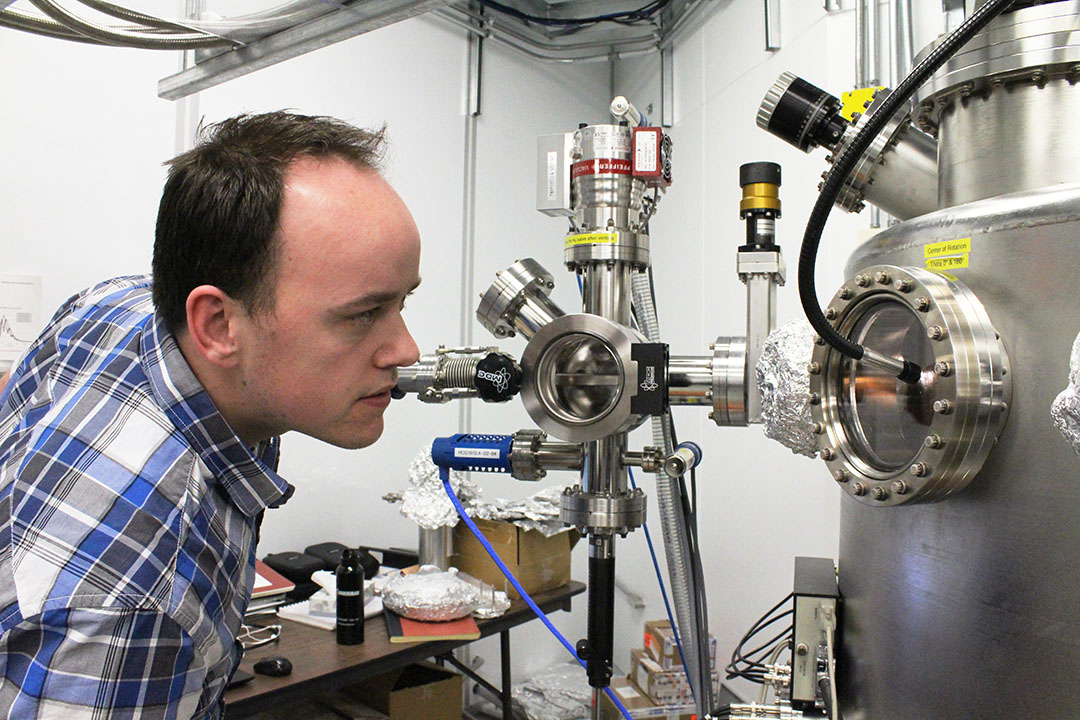
Cutting-edge experiments conducted at the Canadian Light Source (CLS) at the University of Saskatchewan in collaboration with the University of British Columbia and Max Planck Institute for Solid State Research have led to a key advancement in materials science that paves the way for creating more powerful electronic and energy efficient electronic devices in the future.
The findings are published online in a paper in the journal Nature Physics.
Robert Green, assistant professor in the U of S Department of Physics and Engineering Physics, post-doctoral fellow Matthias Hepting at Stanford University and the Max Planck Institute in Germany, and Eva Benckiser, a group leader in solid state spectroscopy at the institute, are the scientists who conceived the project, performed the experiments and analyzed data with a team that also included CLS researchers Feizhou He and Ronny Sutarto.
Green said their experiments involved the study of nickel oxide-based material, one of a group known as “correlated materials” that exhibit complex properties. Individual electrons in correlated materials interact strongly with each other, unlike electrons in simpler materials such as silicon used in electronics today, which basically move freely and independently of other electrons.
This interaction can lead to unique emerging properties that could be harnessed for use in future generations of electronic devices.
The researchers in Germany grew the crystals in extremely thin layers—about one-thousandths the thickness of a human hair—on a neutral substrate material.
Among the interesting properties of the ceramic-like material studied is that at room temperature it conducts electricity, but when cooled to a temperatures of minus-200 Celsius or colder it suddenly becomes a robust insulator.
In addition, the material takes on a unique magnetic property when it’s cooled. At the nanoscale, the magnetism in the crystal structure takes on a distinctive spiral shape.
“What we did here first was to examine these spiral structures at the nano scale, and second, to see if we could tune them a bit to make them do what we wanted—a bit of an engineering aspect to see if we could design some functionality into these materials,” said Green.
“We did a cutting-edge type of experiment at the CLS where we used very specifically tuned X-rays having specific energies that interact strongly with the magnetism in the material.”
What they found was that, as the material was made thinner and thinner—as thin as eight layers of magnetic atoms—researchers could control the magnetism in the atoms to align in a straight line rather than the spiral shape.
“This nano scale control of the magnetism is the really interesting thing, and that’s why our paper is exciting,” said Green. “Alongside that, our collaborators in Germany performed detailed computations to try to understand why this occurs, and they could reproduce this effect with their calculations.”
Now that researchers can explain the experiment and use the theory technique to predict new materials, they can try to design new correlated materials using the same kind of magnetic engineering.
Green cautions that the current science is at a fundamental level, where researchers are trying to understand why the materials have these properties and what they can make the materials do in terms of magnetism. But the long-term goal is to enable the creation of functional devices using similar materials.
“This material family has well defined properties, so they are well suited to these fundamental studies. Ideally, in the future, we can find some related material whose magnetism we can control at room temperature,” said Green. “You can then potentially build next-generation devices that take up less energy, are more powerful, or have entirely different functionalities than present day electronics.”